- 您现在的位置:买卖IC网 > Sheet目录2006 > LTC2600IUFD#PBF (Linear Technology)IC DAC OCTAL R-R 16BIT 20-QFN
LTC2600/LTC2610/LTC2620
5
2600fe
Note 1: Stresses beyond those listed under Absolute Maximum Ratings
may cause permanent damage to the device. Exposure to any Absolute
Maximum Rating condition for extended periods may affect device
reliability and lifetime.
Note 2: Linearity and monotonicity are dened from code kL to code
2N – 1, where N is the resolution and kL is given by kL = 0.016(2N/VREF),
rounded to the nearest whole code. For VREF = 4.096V and N = 16, kL =
256 and linearity is dened from code 256 to code 65,535.
Note 3: Digital inputs at 0V or VCC.
Note 4: DC crosstalk is measured with VCC = 5V and VREF = 4.096V,
with the measured DAC at mid-scale, unless otherwise noted.
Note 5: RL = 2kΩ to GND or VCC.
Note 6: Guaranteed by design and not production tested.
Note 7: Inferred from measurement at code 256 (LTC2600),
code 64 (LTC2610) or code 16 (LTC2620), and at full-scale.
Note 8: VCC = 5V, VREF = 4.096V. DAC is stepped 1/4-scale to 3/4-scale
and 3/4-scale to 1/4-scale. Load is 2k in parallel with 200pF to GND.
Note 9: VCC = 5V, VREF = 4.096V. DAC is stepped ±1LSB between half-
scale and half-scale – 1. Load is 2k in parallel with 200pF to GND.
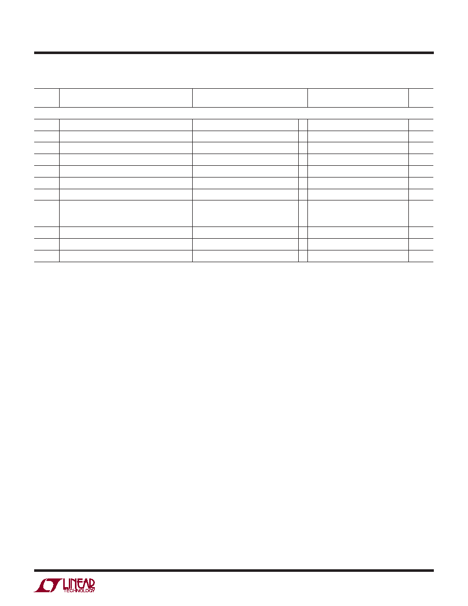
TIMING CHARACTERISTICS The l denotes specications which apply over the full operating temperature
range, otherwise specications are at TA = 25°C. (See Figure 1) (Note 6)
SYMBOL PARAMETER
CONDITIONS
LTC2600/LTC2610/LTC2620
UNITS
MIN
TYP
MAX
VCC = 2.5V to 5.5V
t1
SDI Valid to SCK Setup
l
4ns
t2
SDI Valid to SCK Hold
l
4ns
t3
SCK High Time
l
9ns
t4
SCK Low Time
l
9ns
t5
CS/LD Pulse Width
l
10
ns
t6
LSB SCK High to CS/LD High
l
7ns
t7
CS/LD Low to SCK High
l
7ns
t8
SDO Propagation Delay from SCK Falling Edge
CLOAD = 10pF
VCC = 4.5V to 5.5V
VCC = 2.5V to 5.5V
l
20
45
ns
t9
CLR Pulse Width
l
20
ns
t10
CS/LD High to SCK Positive Edge
l
7ns
SCK Frequency
50% Duty Cycle
l
50
MHz
发布紧急采购,3分钟左右您将得到回复。
相关PDF资料
LTC2602IMS8#TRPBF
IC DAC 16BIT DUAL R-R VOUT 8MSOP
LTC2604IGN-1#TRPBF
IC DAC 16BIT QUAD R-R OUT 16SSOP
LTC2605IGN-1#TRPBF
IC DAC 16BIT OCT I2C 16-SSOP
LTC2606IDD#TRPBF
IC DAC 16BIT I2C V-OUT 10-DFN
LTC2607IDE#TRPBF
IC DAC 16BIT R-R I2C 12-DFN
LTC2609CGN#PBF
IC DAC 16BIT R-R QUAD 16SSOP
LTC2621IDD-1#PBF
IC DAC 12BIT R-R 10-DFN
LTC2630HSC6-LZ12#TRPBF
IC DAC 12BIT R-R SC70-6
相关代理商/技术参数
LTC2600IUFD#TRPBF
功能描述:IC DAC OCTAL R-R 16BIT 20-QFN RoHS:是 类别:集成电路 (IC) >> 数据采集 - 数模转换器 系列:- 产品培训模块:Data Converter Fundamentals
DAC Architectures 标准包装:750 系列:- 设置时间:7µs 位数:16 数据接口:并联 转换器数目:1 电压电源:双 ± 功率耗散(最大):100mW 工作温度:0°C ~ 70°C 安装类型:表面贴装 封装/外壳:28-LCC(J 形引线) 供应商设备封装:28-PLCC(11.51x11.51) 包装:带卷 (TR) 输出数目和类型:1 电压,单极;1 电压,双极 采样率(每秒):143k
LTC2601CDD
功能描述:IC DAC 16BIT SGL R-R VOUT 10DFN RoHS:否 类别:集成电路 (IC) >> 数据采集 - 数模转换器 系列:- 产品培训模块:LTC263x 12-, 10-, and 8-Bit VOUT DAC Family 特色产品:LTC2636 - Octal 12-/10-/8-Bit SPI VOUT DACs with 10ppm/°C Reference 标准包装:91 系列:- 设置时间:4µs 位数:10 数据接口:MICROWIRE?,串行,SPI? 转换器数目:8 电压电源:单电源 功率耗散(最大):2.7mW 工作温度:-40°C ~ 85°C 安装类型:表面贴装 封装/外壳:14-WFDFN 裸露焊盘 供应商设备封装:14-DFN-EP(4x3) 包装:管件 输出数目和类型:8 电压,单极 采样率(每秒):*
LTC2601CDD#PBF
功能描述:IC DAC 16BIT SGL R-R VOUT 10DFN RoHS:是 类别:集成电路 (IC) >> 数据采集 - 数模转换器 系列:- 产品培训模块:Lead (SnPb) Finish for COTS
Obsolescence Mitigation Program 标准包装:50 系列:- 设置时间:4µs 位数:12 数据接口:串行 转换器数目:2 电压电源:单电源 功率耗散(最大):- 工作温度:-40°C ~ 85°C 安装类型:表面贴装 封装/外壳:8-TSSOP,8-MSOP(0.118",3.00mm 宽) 供应商设备封装:8-uMAX 包装:管件 输出数目和类型:2 电压,单极 采样率(每秒):* 产品目录页面:1398 (CN2011-ZH PDF)
LTC2601CDD#TR
功能描述:IC DAC 16BIT SGL R-R VOUT 10DFN RoHS:否 类别:集成电路 (IC) >> 数据采集 - 数模转换器 系列:- 产品培训模块:LTC263x 12-, 10-, and 8-Bit VOUT DAC Family 特色产品:LTC2636 - Octal 12-/10-/8-Bit SPI VOUT DACs with 10ppm/°C Reference 标准包装:91 系列:- 设置时间:4µs 位数:10 数据接口:MICROWIRE?,串行,SPI? 转换器数目:8 电压电源:单电源 功率耗散(最大):2.7mW 工作温度:-40°C ~ 85°C 安装类型:表面贴装 封装/外壳:14-WFDFN 裸露焊盘 供应商设备封装:14-DFN-EP(4x3) 包装:管件 输出数目和类型:8 电压,单极 采样率(每秒):*
LTC2601CDD#TRPBF
功能描述:IC DAC 16BIT SGL R-R VOUT 10DFN RoHS:是 类别:集成电路 (IC) >> 数据采集 - 数模转换器 系列:- 产品培训模块:LTC263x 12-, 10-, and 8-Bit VOUT DAC Family 特色产品:LTC2636 - Octal 12-/10-/8-Bit SPI VOUT DACs with 10ppm/°C Reference 标准包装:91 系列:- 设置时间:4µs 位数:10 数据接口:MICROWIRE?,串行,SPI? 转换器数目:8 电压电源:单电源 功率耗散(最大):2.7mW 工作温度:-40°C ~ 85°C 安装类型:表面贴装 封装/外壳:14-WFDFN 裸露焊盘 供应商设备封装:14-DFN-EP(4x3) 包装:管件 输出数目和类型:8 电压,单极 采样率(每秒):*
LTC2601CDD-1#PBF
功能描述:IC DAC 16BIT R-R 10-DFN RoHS:是 类别:集成电路 (IC) >> 数据采集 - 数模转换器 系列:- 产品培训模块:Lead (SnPb) Finish for COTS
Obsolescence Mitigation Program 标准包装:50 系列:- 设置时间:4µs 位数:12 数据接口:串行 转换器数目:2 电压电源:单电源 功率耗散(最大):- 工作温度:-40°C ~ 85°C 安装类型:表面贴装 封装/外壳:8-TSSOP,8-MSOP(0.118",3.00mm 宽) 供应商设备封装:8-uMAX 包装:管件 输出数目和类型:2 电压,单极 采样率(每秒):* 产品目录页面:1398 (CN2011-ZH PDF)
LTC2601CDD-1#TRPBF
功能描述:IC DAC 16BIT SGL R-R VOUT 10DFN RoHS:是 类别:集成电路 (IC) >> 数据采集 - 数模转换器 系列:- 标准包装:2,400 系列:- 设置时间:- 位数:18 数据接口:串行 转换器数目:3 电压电源:模拟和数字 功率耗散(最大):- 工作温度:-40°C ~ 85°C 安装类型:表面贴装 封装/外壳:36-TFBGA 供应商设备封装:36-TFBGA 包装:带卷 (TR) 输出数目和类型:* 采样率(每秒):*
LTC2601IDD
功能描述:IC DAC 16BIT SGL R-R VOUT 10DFN RoHS:否 类别:集成电路 (IC) >> 数据采集 - 数模转换器 系列:- 产品培训模块:LTC263x 12-, 10-, and 8-Bit VOUT DAC Family 特色产品:LTC2636 - Octal 12-/10-/8-Bit SPI VOUT DACs with 10ppm/°C Reference 标准包装:91 系列:- 设置时间:4µs 位数:10 数据接口:MICROWIRE?,串行,SPI? 转换器数目:8 电压电源:单电源 功率耗散(最大):2.7mW 工作温度:-40°C ~ 85°C 安装类型:表面贴装 封装/外壳:14-WFDFN 裸露焊盘 供应商设备封装:14-DFN-EP(4x3) 包装:管件 输出数目和类型:8 电压,单极 采样率(每秒):*